Although ultrafast lasers have been around for decades, industrial applications have grown rapidly in the past two decades. In 2019, the market value of ultrafast laser material processing was approximately US$460 million, with a compound annual growth rate of 13%. Application areas where ultrafast lasers have been successfully used to process industrial materials include photomask fabrication and repair in the semiconductor industry as well as silicon dicing, glass cutting/scribing and (indium tin oxide) ITO film removal in consumer electronics such as mobile phones and tablets , piston texturing for the automotive industry, coronary stent manufacturing and microfluidic device manufacturing for the medical industry.
01 Photomask manufacturing and repair in the semiconductor industry
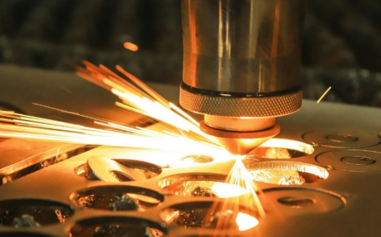
Ultrafast lasers were used in one of the earliest industrial applications in materials processing. IBM reported the application of femtosecond laser ablation in photomask production in the 1990s. Compared with nanosecond laser ablation, which can produce metal spatter and glass damage, femtosecond laser masks show no metal spatter, no glass damage, etc. The advantages. This method is used to produce integrated circuits (ICs). Producing an IC chip may require up to 30 masks and cost >$100,000. Femtosecond laser processing can process lines and points below 150nm.
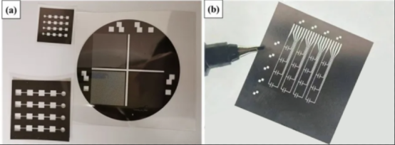
Figure 1. Photomask fabrication and repair
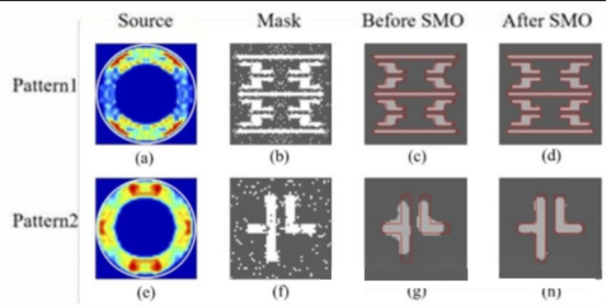
Figure 2. Optimization results of different mask patterns for extreme ultraviolet lithography
02 Silicon cutting in the semiconductor industry
Silicon wafer dicing is a standard manufacturing process in the semiconductor industry and is typically performed using mechanical dicing. These cutting wheels often develop microcracks and are difficult to cut thin (e.g. thickness < 150 μm) wafers. Laser cutting of silicon wafers has been used in the semiconductor industry for many years, especially for thin wafers (100-200μm), and is carried out in multiple steps: laser grooving, followed by mechanical separation or stealth cutting (i.e. infrared laser beam inside the silicon scribing) followed by mechanical tape separation. The nanosecond pulse laser can process 15 wafers per hour, and the picosecond laser can process 23 wafers per hour, with higher quality.
03 Glass cutting/scribing in the consumable electronics industry
Touch screens and protective glasses for mobile phones and laptops are getting thinner and some geometric shapes are curved. This makes traditional mechanical cutting more difficult. Typical lasers typically produce poor cut quality, especially when these glass displays are stacked 3-4 layers and the top 700 μm thick protective glass is tempered, which can break with localized stress. Ultrafast lasers have been shown to be able to cut these glasses with better edge strength. For large flat panel cutting, the femtosecond laser can be focused onto the back surface of the glass sheet, scratching the inside of the glass without damaging the front surface. The glass can then be broken using mechanical or thermal means along the scored pattern.
Figure 3. Picosecond ultrafast laser glass special-shaped cutting
04 Piston textures in the automotive industry
Lightweight car engines are made of aluminum alloys, which are not as wear-resistant as cast iron. Studies have found that femtosecond laser processing of car piston textures can reduce friction by up to 25% because debris and oil can be effectively stored.
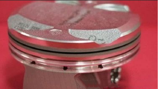
Figure 4. Femtosecond laser processing of automobile engine pistons to improve engine performance
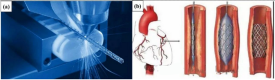
05 Coronary stent manufacturing in the medical industry
Millions of coronary stents are implanted into the body’s coronary arteries to open a channel for blood to flow into otherwise clotted vessels, saving millions of lives every year. Coronary stents are typically made from metal (e.g., stainless steel, nickel-titanium shape memory alloy, or more recently cobalt-chromium alloy) wire mesh with a strut width of approximately 100 μm. Compared to long-pulse laser cutting, the advantages of using ultrafast lasers to cut brackets are high cut quality, better surface finish, and less debris, which reduces post-processing costs.
06 Microfluidic device manufacturing for the medical industry
Microfluidic devices are commonly used in the medical industry for disease testing and diagnosis. These are typically manufactured by micro-injection molding of individual parts and then bonding using gluing or welding. Ultrafast laser fabrication of microfluidic devices has the advantage of producing 3D microchannels within transparent materials such as glass without the need for connections. One method is ultrafast laser fabrication inside a bulk glass followed by wet chemical etching, and another is femtosecond laser ablation inside glass or plastic in distilled water to remove debris. Another approach is to machine channels into the glass surface and seal them with a glass cover via femtosecond laser welding.
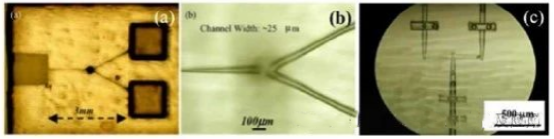
Figure 6. Femtosecond laser-induced selective etching to prepare microfluidic channels inside glass materials
07 Micro drilling of injector nozzle
Femtosecond laser microhole machining has replaced micro-EDM at many companies in the high-pressure injector market due to greater flexibility in changing flow hole profiles and shorter machining times. The ability to automatically control the focus position and tilt of the beam through a precessing scan head has led to the design of aperture profiles (e.g., barrel, flare, convergence, divergence) that can promote atomization or penetration in the combustion chamber. Drilling time depends on the ablation volume, with drill thickness of 0.2 – 0.5 mm and hole diameter of 0.12 – 0.25 mm, making this technique ten times faster than micro-EDM. Microdrilling is performed in three stages, including roughing and finishing of through-pilot holes. Argon is used as an auxiliary gas to protect the borehole from oxidation and to shield the final plasma during the initial stages.
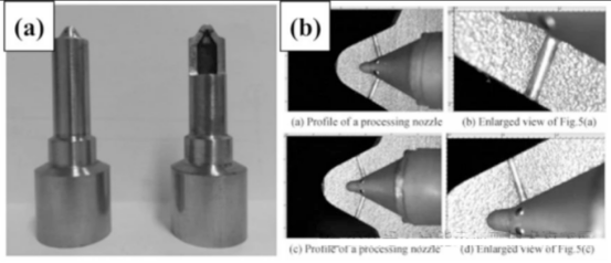
Figure 7. Femtosecond laser high-precision processing of inverted taper hole for diesel engine injector
08 Ultra-fast laser texturing
In recent years, in order to improve machining accuracy, reduce material damage, and increase processing efficiency, the field of micromachining has gradually become a focus of researchers. Ultrafast laser has various processing advantages such as low damage and high precision, which has become the focus of promoting the development of processing technology. At the same time, ultrafast lasers can act on a variety of materials, and laser processing material damage is also a major research direction. Ultrafast laser is used to ablate materials. When the energy density of the laser is higher than the ablation threshold of the material, the surface of the ablated material will show a micro-nano structure with certain characteristics. Research shows that this special surface Structure is a common phenomenon that occurs when laser processing materials. The preparation of surface micro-nano structures can improve the properties of the material itself and also enable the development of new materials. This makes the preparation of surface micro-nano structures by ultrafast laser a technical method with important development significance. Currently, for metal materials, research on ultrafast laser surface texturing can improve metal surface wetting properties, improve surface friction and wear properties, enhance coating adhesion, and directional proliferation and adhesion of cells.
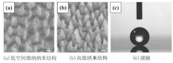
Figure 8. Superhydrophobic properties of laser-prepared silicon surface
As a cutting-edge processing technology, ultrafast laser processing has the characteristics of small heat-affected zone, non-linear process of interaction with materials, and high-resolution processing beyond the diffraction limit. It can realize high-quality and high-precision micro-nano processing of various materials. and three-dimensional micro-nano structure fabrication. Achieving laser manufacturing of special materials, complex structures and special devices opens up new avenues for micro-nano manufacturing. At present, femtosecond laser has been widely used in many cutting-edge scientific fields: femtosecond laser can be used to prepare various optical devices, such as microlens arrays, bionic compound eyes, optical waveguides and metasurfaces; using its high precision, high resolution and With three-dimensional processing capabilities, femtosecond laser can prepare or integrate microfluidic and optofluidic chips such as microheater components and three-dimensional microfluidic channels; in addition, femtosecond laser can also prepare different types of surface micro-nanostructures to achieve anti-reflection , anti-reflection, super-hydrophobic, anti-icing and other functions; not only that, femtosecond laser has also been applied in the field of biomedicine, showing outstanding performance in fields such as biological micro-stents, cell culture substrates and biological microscopic imaging. Broad application prospects. At present, the application fields of femtosecond laser processing are expanding year by year. In addition to the above-mentioned micro-optics, microfluidics, multi-functional micro-nanostructures and biomedical engineering applications, it also plays a huge role in some emerging fields, such as metasurface preparation. , micro-nano manufacturing and multi-dimensional optical information storage, etc.
Post time: Apr-17-2024